A Novel SOI-LDMOSFET With Superior Electrical Performances

- Citation Author(s):
- Submitted by:
- Mohammadreza Ghamkhar
- Last updated:
- DOI:
- 10.21227/e2s1-ay90
- Data Format:
Abstract
In this paper, a novel silicon-on-insulator (SOI) lateral-double-diffused metal-oxide-semiconductor field-effect transistor (LDMOSFET) is presented. Changing charge distribution leads to lower electric field crowding and increased breakdown voltage (VBR). For modifying charge distribution, a metal region (COLUMN) and an air layer inside the transistor are utilized. On the other the floating-body effect and impact ionization generate excess holes that are amplified by the parasitic bipolar junction transistor (BJT) in SOI-LDMOSFET that degrade the transistor performance. For that matter, a silicon layer below the BOX, connected to the channel region via the COLUMN has been replaced in order to reduce the hole concentration in the channel and control the BJT effect significantly. In order to achieve the best results, the COLUMN and the silicon layer under the BOX location and dimensions are optimized carefully. DC and radio frequency characteristics of the proposed structure are analyzed by 2-D numerical simulation and compared with conventional SOI-LDMOSFET (C-SOI-LDMOSFET) characteristics. The VBR of the proposed structure improves by 229% compared with that of the C-SOI-LDMOSFET structure. Although drain current of the proposed structure reduces slightly, 220% improvement in maximum output power density of the device is achieved due to high enhancement of the VBR. Also, the proposed structure leads to the improvement of maximum oscillation frequency, maximum available gain, and self-heating effects of the device. As a result, the proposed structure has superior electrical performances in comparison with the similar device based on the conventional structure.
Instructions:
Nowadays, silicon-on-insulator (SOI) technology attracts much attention in high-speed and low-powerconsumption applications. SOI structures have important advantages such as low leakage current, higher switching speed, considerable reduction in parasitic capacitance (low junction capacitance) for power and high voltage ICs, latch-up immunity, and improved device isolation because of utilizing the buried oxide (BOX) [1]-[2]. Furthermore, they have the advantage of being compatible with mainstream CMOS processing. The SOI CMOS is a low-cost technology that can be used for radio frequency (RF) integrated circuits because of its ability to merge RF circuits and digital logic on a single chip [3]–[5]. In many researches, lateral double-diffused MOSFETs (LDMOSFET) on SOI have been attracted because the processes are easy to integrate with other devices and are also compatible with the BiCMOS technology [6]. Two important advantages of the SOI-LDMOSFET are low ON-resistance and high breakdown voltage. However, the parasitic bipolar junction transistor (BJT) due to the floatingbody effect is more detrimental in such devices and must be controlled. Various solutions have been proposed to reduce the floating-body effect and the parasitic BJT effect [7]–[10].
The floating-body effect and impact ionization generate excess holes that are amplified with the parasitic BJT in the SOI-LDMOSFET and degrade their performance. If we could absorb the generated holes from the impact ionization mechanism in the SOI-LDMOSFET, that time, complete absence of the hole concentration in the channel and a significantly diminished BJT effect without affecting the ON-state current occur. In a paper has proposed a silicon germanium (SiGe) window under the channel region to reduce the buried oxide thickness in which the SiGe window under the channel region can absorb and recombine the impact generated holes to suppress the floating-body effect and improve the breakdown voltage [11].
In SOI technology, SOI lateral double-diffused metal–oxide–semiconductor fielde-ffect transistor (LDMOSFET) many times has been investigated and taken into consideration. As the carriers placed in the inversion layer of a SOI-LDMOSFET structure have a wave function that extends into the oxide, their mobility, which is also referred to as surface mobility, is lower than half of the bulk material mobility. Higher mobility leads to higher transconductance (gm), current, and frequency parameters of the device [12].
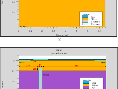
On account of the various progresses in analyzing and improving the SOI-LDMOSFET characteristics, a number of important investigations for the SOI-LDMOSFET structure have been reported. The charge distribution plays an important role in determining device characteristics [13]–[16]. In a paper for changing the charge distribution, a metal region is used in the BOX of the proposed structure [17]. Among the features of our paper is to modify charge distribution of the bulk and specially channel region in order to lower the electric field of the device and improve the VBR. For changing the charge distribution, a metal column (COLUMN) is used in the BOX of the proposed structure , which is only from the air, also in this paper, I have proposed a silicon layer under the BOX layer that silicon layer through the metal column can absorb and recombine the impact generated holes to suppress the floating-body effect [18]. In addition, the optimum value of doping and silicon layer height under the BOX layer is determined that with lower hole concentration in the channel region leads to the higher breakdown voltage.
In this paper, I have focused on the parasitic BJT effect too and also have investigated the self-heating effect as another disadvantage in the SOI-LDMOSFET. The self-heating effect occurs due to the poor thermal conductivity of the buried oxide and degrades the device performance in the SOI technology. In previous efforts, many novel devices have been proposed to control these penalties [19]–[21], such as partial SOI in which the buried oxide is patterned to have a silicon window that connects the active region to the substrate offering a heat conduction path [19]. Hence, reduced self-heating effects and high breakdown voltage can be achieved [19].
Thus, in this paper, I introduce a novel SOI-LDMOSFET structure with a COLUMN in the BOX of transistor that all of the BOX is air and with a silicon layer under the BOX. After utilizing the COLUMN and silicon layer under a BOX full of air in the structure and optimizing their location and dimensions, the proposed SOI-LDMOSFET characteristics such as hole concentration, electric field distribution, VBR, potential distribution, drain current (ID), output power density, unilateral power gain (U), maximum available gain (MAG), and current gain (fT ) are analyzed. The aim of the proposed structure is to get a high-power and high-speed device also the proposed structure set can alleviate self-heating and control the floating-body effect significantly. Using 2-D device simulation, I have demonstrated that proposed structure, considerable improvements in the breakdown voltage, self-heating effects, and gate capacitance are achieved.
 189 views





0000